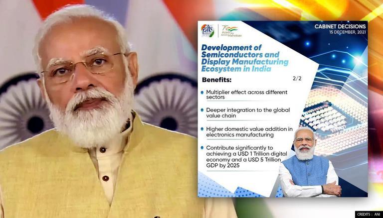
India semiconductor mission: Union Information Technology Minister Ashwini Vaishnaw launched the India Semiconductor Mission on December 29, 2021. Under the scheme, the companies that are interested in developing the semiconductors and display manufacturing ecosystem in India can start applying from January 1st.
The companies will be able to enjoy the Rs 76,000-crore incentives under the mission that have been earmarked by the Centre for the development of the semiconductors and display manufacturing ecosystem in India.
The IT Minister said that the schemes under the mission have been notified and uploaded on the website. "A portal for the same has been prepared for receiving the applications. Come January 1, 2022, onwards, we will start receiving the applications," the Minister said.
What is India Semiconductor Mission?
• India Semiconductor Mission is a specialised business division that has been created within the Digital India Corporation. The mission aims to build a vibrant semiconductor and display ecosystem to enable India’s emergence as a global hub for electronics manufacturing and design.
• The mission will have the autonomy to decide the appropriate technology mix, applications, node generation, capacity and propose the structure and quantum of fiscal support for the selected applicants.

• The mission will be able to negotiate with the applicants under the semiconductor fab scheme and the display fab scheme.
• The semiconductor fab scheme and display fab scheme are among the four schemes notified by the Ministry of Electronics and Information Technology on December 21.
All four schemes are as follows-
Scheme for setting up semiconductor fab: The centre has approved financial support of up to 50 percent of the project cost for setting up certain variants of silicon-based semiconductor fab in India. The financial support will be provided to the scheme for six years from the date of approval. The semiconductor fabs set up in India will be eligible for a purchase preference in the procurement of electronic products by the government.
Scheme for setting up display fabs: The centre has earmarked financial support of up to Rs 12,000 crores per fab under the scheme for setting up display fabs in India. This scheme aims to attract large investments in manufacturing TFT LCD or AMOLED-based display panels.
Scheme for Setting up of Compound Semiconductors / Silicon Photonics / Sensors: The Scheme for Setting up of Compound Semiconductors / Silicon Photonics / Sensors (including MEMS) Fabs and Semiconductor ATMP / OSAT facilities in the country will extend fiscal support of 30 percent of capital expenditure to approved units. At least 15 such units of Compound Semiconductors and Semiconductor Packaging will be established under this scheme.
Design Linked Incentive (DLI) Scheme: The Design Linked Incentive (DLI) Scheme will offer an incentive of up to 50 percent of eligible expenditure and product deployment linked incentive of 4-6 percent on net sales for five years.
Do You Know!What is fab?A fab is short for a fabrication plant where raw silicon wafers are processed and transformed into integrated circuits. What is a semiconductor?A semiconductor is a material product that is usually made up of silicon, which conducts electricity more than an insulator, such as glass, but less than a pure conductor, such as metallic copper or aluminum. The electrical conductivity of the semiconductor can be altered with the introduction of impurities to meet the specific needs of the electronic component in which it resides. |
Background
The Union Cabinet had approved all these four schemes on December 15, 2021. The centre has committed to provide financial support of Rs 2.30 trillion to position India as a global hub for electronics manufacturing.


